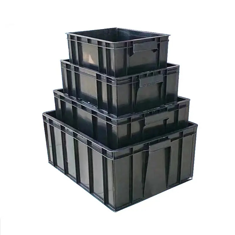
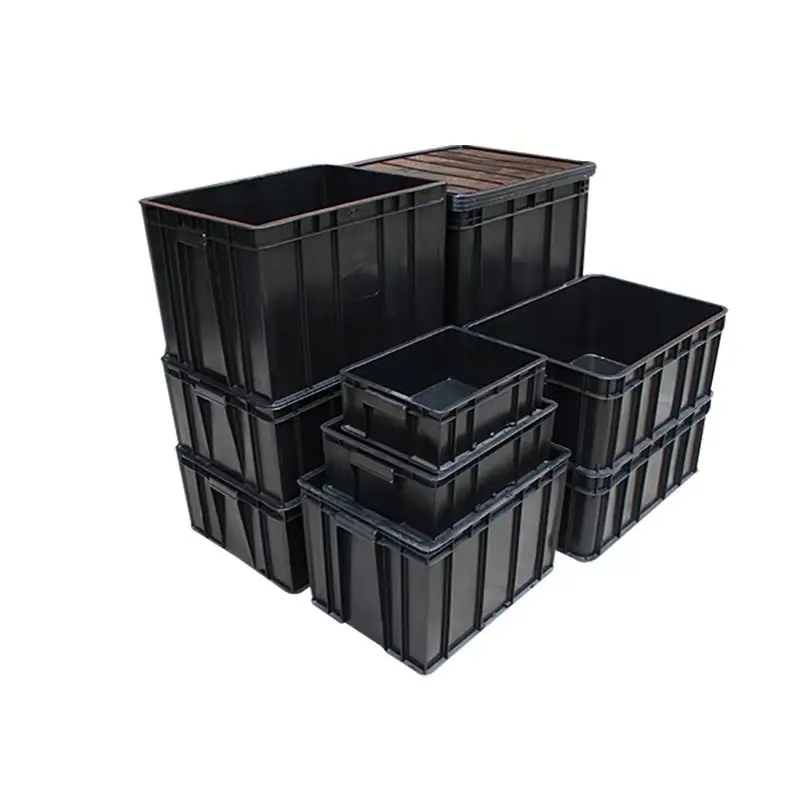
Here is the table summarizing the ESD box dimensions:
Outer Size (mm) Inner Size (mm)
252×175×75 223×160×69
303×208×85 267×180×78
380×240×100 340×220×90
350×265×125 315×235×120
410×305×155 380×275×145
480×355×170 445×320×165
480×355×220 445×320×210
540×420×300 500×380×290
545×415×370 500×380×360
600×500×360 560×460×350
600×500×400 560×460×390
600×500×300 560×460×290
620×425×155 580×390×145
620×425×315 580×390×308
615×425×250 580×390×240
620×425×200 580×390×190
530×370×205 475×330×198
560×430×145 515×385×138
600×500×150 560×455×140
585×405×175 538×360×168
390×370×230 360×340×220
600×500×340 573×470×327
The Critical Importance of Using ESD Protective Boxes in Electronics Manufacturing
In today's technology-driven world, electrostatic discharge (ESD) poses a silent but significant threat to electronic components during manufacturing, storage, and transportation. ESD protective boxes,
such as those listed in the size chart above, serve as the first line of defense against this invisible hazard. These specialized containers are engineered to safeguard sensitive electronics from damage caused by static electricity,
ensuring product reliability and reducing costly waste. This article explores the science behind ESD, the design principles of protective packaging, and the operational advantages these boxes provide across industries.
1. The Hidden Danger of Electrostatic Discharge
Electrostatic discharge occurs when a sudden flow of electricity passes between two charged objects,
often with voltages exceeding thousands of volts. While humans rarely feel discharges below 3,000V,
integrated circuits can be damaged by as little as 10V. Modern microelectronics, with their nanometer-scale transistors, are particularly vulnerable.
A single ESD event can cause latent defects that may not immediately fail but degrade performance over time, leading to premature field failures.
Industry studies suggest that ESD accounts for 8-33% of all electronic component losses annually, costing manufacturers billions.
2. Engineering Principles of ESD Boxes
The effectiveness of ESD boxes lies in their multi-layered design:
Conductive Materials: Carbon-loaded polypropylene or polyethylene provides surface resistance of 10³-10⁶ ohms, allowing controlled charge dissipation.
Structural Design: The precise dimensional tolerances (as shown in the size chart) ensure components remain immobilized during transit,
preventing triboelectric charging from movement.
Shielding Capability: High-grade ESD boxes incorporate metallized layers that create a Faraday cage effect, deflecting external electrostatic fields.
Environmental Protection: Many designs offer moisture resistance (often <0.5% water absorption) and anti-dust properties while maintaining accessibility through hinged lids.
3. Operational Advantages Across Industries
Semiconductor Manufacturing
In cleanroom environments, the 600×500×400mm boxes protect wafer carriers during inter-process transfers,
with their 560×460×390mm internal dimensions accommodating standard FOUP containers.
The smooth interior surfaces prevent particle generation.
Automotive Electronics
The 380×240×100mm size is ideal for ECU components,
providing both ESD protection and mechanical shock absorption during automotive assembly line handling.
Aerospace Applications
Larger boxes like the 540×420×300mm version (500×380×290mm internal) are used for avionics,
meeting MIL-STD-1686C standards for static control in high-vibration environments.
4. Cost-Benefit Analysis
While ESD boxes cost 20-50% more than standard packaging, they deliver measurable ROI:
A 300mm wafer protected in a 620×425×315mm box represents $20,000-$50,000 in saved potential losses
Reduction in warranty claims by up to 17% for consumer electronics manufacturers
Compliance with international standards (ANSI/ESD S20.20, IEC 61340-5-1) avoids non-conformance penalties
5. Selection Guidelines
Choosing the right size is critical:
Allow 5-10mm clearance on all sides (note the consistent 20-40mm wall thickness in our chart)
For PCB storage, select boxes where the inner height exceeds board thickness by ≥15mm
Stackable designs (like the 600×500 series) optimize warehouse space utilization
As electronic components continue to shrink in size while growing in complexity,
the role of ESD protective packaging becomes ever more crucial. The comprehensive size range available
—from compact 252×175×75mm units for microcomponents to expansive 600×500×400mm systems for bulk storage
—ensures that every stage of the electronics value chain can be protected. By implementing proper ESD control measures including these specialized boxes,
manufacturers can significantly improve yield rates, enhance product longevity, and maintain their reputation for quality in an increasingly competitive marketplace.
Investing in the right ESD solution isn't just about preventing damage
—it's about ensuring the reliable operation of the technologies that power our modern world.
The dimensional precision and material science behind these unassuming boxes represent a critical intersection of physics, engineering, and practical manufacturing wisdom.